AS(AmericanSamoa) pcb manufacturing,multilayer pcb manufacturing in AS(AmericanSamoa)
- Author:Admin
- Time:2023-11-27
- Browse:
We have extensive experience in the manufacturing of printed circuit boards (PCBs) that are tailored to meet the diverse needs of different industries and applications. Our specialization lies in the production of a wide range of PCB types, including 1-20 layer high-density impedance, blind/buried, HDI, high frequency, high TG, aluminum, and heavy copper PCBs. These PCBs have gained widespread popularity and are extensively utilized in fields such as communication, medical equipment, consumer electronics, vehicle electronics, and more. We are dedicated to upholding the highest standards of quality and employ advanced manufacturing techniques to ensure that our PCBs adhere to the stringent requirements of these industries. By offering reliable and high-performance solutions, we aim to provide our customers with the best PCB products available.
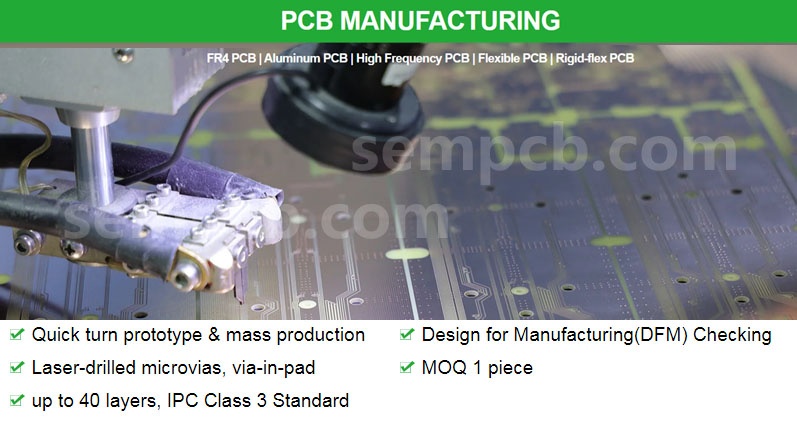
pcb manufacturing Types
HDI PCB manufacturing
HDI PCBs are a type of multilayer PCB that utilizes advanced technologies to achieve higher circuit density and miniaturization. They incorporate microvias and high-density routing to accommodate complex and densely packed components.
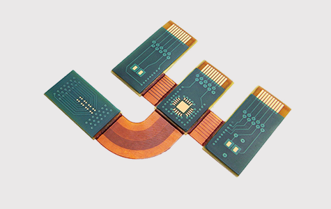
Rigid-Flex PCB manufacturing
Aluminum PCB, also known as Metal Core PCB, is a type of printed circuit board that uses an aluminum base material. It possesses unique characteristics and application advantages compared to traditional substrate materials such as FR-4. The structure of a
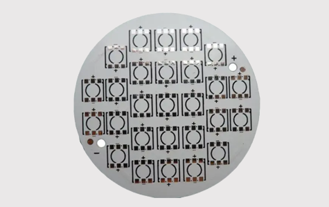
Aluminum PCB manufacturing
Aluminum PCB, also known as Metal Core PCB, is a type of printed circuit board that uses an aluminum base material. It possesses unique characteristics and application advantages compared to traditional substrate materials such as FR-4.
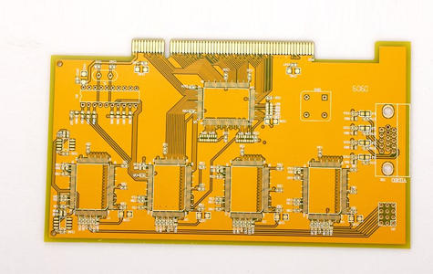
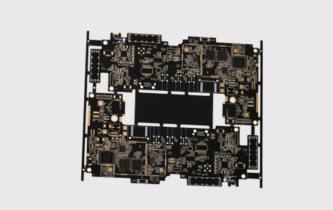
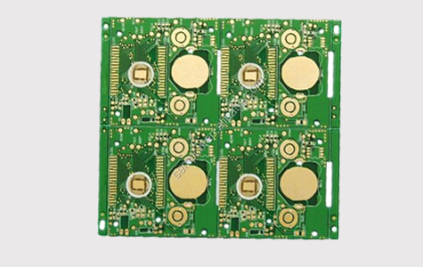
Multilayer PCB manufacturing
Multilayer PCB (Printed Circuit Board) refers to a type of PCB that consists of multiple layers of conductive traces and insulating material stacked together. Unlike single-layer or double-layer PCBs, which have only one or two layers of conductive materi
Heavy Copper PCB manufacturing
Heavy Copper PCB refers to a type of printed circuit board that features a significantly thicker copper layer compared to standard PCBs. The copper thickness in heavy copper PCBs typically ranges from 3 ounces (105 micrometers) to 20 ounces (700 micromete
Steps of the PCB manufacturing process
PCB production process mainly includes design, graphic conversion, plate making, etching, drilling, coating, welding, testing and cleaning steps.Design phase
The design stage is the starting point of PCB production, and the circuit schematic and PCB layout are designed through CAD software to determine the size of the PCB board, the routing method, the size of the pad and other information.
Graphic conversion phase
After the design is completed, the circuit schematics and PCB layout diagrams need to be converted into Gerber files for processes such as plate making and etching.
Plate making stage
Plate making is the core link in PCB production, by converting the Gerber file into a photoresist film, and then through exposure, development and other processes to transfer the photoresist film graphics to the copper foil, to make the PCB board line and graphics.
Etching stage
Etching is the process of removing the unnecessary copper foil part, by soaking the copper foil after plate making in the etching agent, waiting for a certain time, the excess copper foil is etched away, forming the PCB circuit and graphics.
Drilling stage
Drilling refers to drilling a variety of holes on the PCB board, including pad holes, positioning holes, installation holes, and so on. Drilling requires the use of a drill press or drill machine to operate.
Coating stage
Coating is to remove the photoresist film on the copper-clad plate, and then cover a layer of welding film through the process of drying, exposure, etc., in order to carry out subsequent welding operations.
Welding phase
Welding is the process of installing components to the PCB board and welding them. Soldering iron or welding equipment is required during the welding process.
Detection phase
Inspection is the process of quality inspection of welded PCB board, mainly including AOI inspection, X-ray inspection, ICT inspection and so on.
Cleaning phase
Cleaning is the process of cleaning the welded PCB board for subsequent packaging and assembly operations.
pcb manufacturing Why Choose Semshine
Customer service
A special customer service team contacts customer, offers quick response and provides return and refund service.
Delivery
Before delivery, the item number, customer code, quantity and consignee etc must be fully checked by the PQA.
Test of finish product
Open/short, visual inspection and physical testing.Flying probe,ICT,and functional testing.
Control in Manufacturing
The factory has advanced automatic production line which reduces manual damage to boards.
Pre-production Arrangement
The engineer checks the customer's design information, makes the production documents twice and is confirmed by the customer.
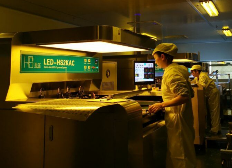
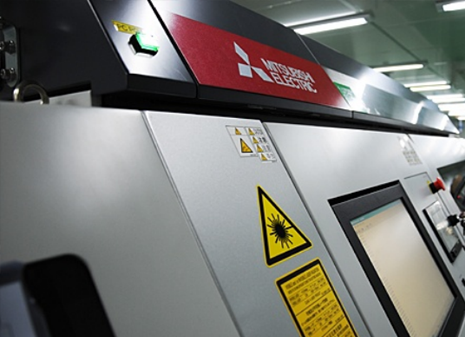
PCB manufacturing workshop
-
 PCB manufacturing workshop
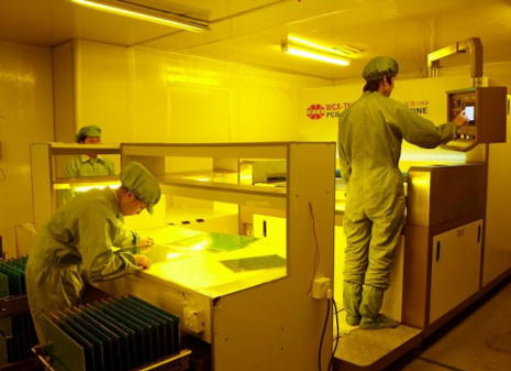
-
 PCB manufacturing workshop
-
 PCB manufacturing workshop
-
 PCB manufacturing workshop
PCB Manufacturer Capabilities
|
Category |
Description |
Capability |
|
File Formats |
Gerber files- preferred |
Gerber file 274-X or ODB++ |
|
Drill file |
3.3 leading mm |
|
|
Size |
Max. finished PCB dimensions |
400mm x 1200mm – Single/ Double-sided |
|
600mm x 700mm – Multilayer |
||
|
Board Thickness |
Standard |
1.6mm ±10% |
|
Min. |
0.6mm ±10% |
|
|
Max. |
3.2mm ±10% |
|
|
Bow and twist |
0.50% |
|
|
Copper Thickness |
Outer Cu weight |
0.5oz-12oz |
|
Inner Cu weight |
0.5oz-12oz |
|
|
Laminate Materials |
FR4(KB, ILM, Shengyi, Huazheng new material ) , |
|
|
Board Cutting |
Max. number of layers |
20 |
|
Min. thickness for inner layers (Cu thickness are |
0.05mm |
|
|
Drilling |
Min. size |
0.20mm |
|
Max. size |
6.00mm |
|
|
Drill Deviation |
±0.075mm |
|
|
NPTH hole tolerance |
±0.05mm |
|
|
Angle of Countersink |
45° |
|
|
PTH |
Min. hole size |
0.20mm |
|
Aspect ratio |
8:1 |
|
|
Etching |
Trace width tolerance |
±20% |
|
Min. trace width / space (1oz finished Cu weight |
75um/75um (3mil/3mil) |
|
|
Min. trace width / space (1oz finished Cu weight |
89um/89um (3.5mil/3.5mmil) |
|
|
Min. trace width / space (2oz finished Cu weight) |
150um/150um (6mil/6mil) |
|
|
Solder Mask |
Color |
Green,White,Black,Red,Blue,Etc. |
|
Min. solder mask clearance |
3mil |
|
|
Thickness |
Line angle:8um(min),Linear plane:10um(min), |
|
|
Silkscreen |
Color |
White,Black,Etc. |
|
Min. trace width |
100um 4mil |
|
|
Min. size |
0.7mm 28mil |
|
|
Test |
AOI |
100% |
|
Flying Probe Tester |
Sample 100% |
|
|
E-test |
Mass order 100% |
|
|
Controlled Impedance |
Tolerance |
+/-10% |
|
Impedance tester |
Test impedance module |
|
|
Profile |
Tolerance |
±0.10mm |
|
V—CUT Depth |
±0.10mm |
|
|
V—CUT angle deviation |
30° |
|
|
Semi-hole |
Minimum half hole:0.40mm |
|
|
Surface Finish |
HASL,Immersion gold(ENIG),OSP |
|
Disclaimer: All works (images, text, audio, and video) on this website are compiled from internet sources for the purpose of learning and communication among users. If your rights have been infringed, please contact the administrator to request removal.
https://www.sempcb.com/
Related Blog
- ZW(Zimbabwe) pcb manufacturing,multilayer pcb...
- VE(Venezuela) pcb manufacturing,multilayer pc...
- UM(USMinorOutlyingIslands) pcb manufacturing,...
- AE(UnitedArabEmirates) pcb manufacturing,mult...
- TM(Turkmenistan) pcb manufacturing,multilayer...
- TJ(Tajikistan) pcb manufacturing,multilayer p...
- SH(St.Helena) pcb manufacturing,multilayer pc...
- ZA(SouthAfrica) pcb manufacturing,multilayer ...
- ZR(Zaire) pcb manufacturing,multilayer pcb ma...
- ZM(Zambia) pcb manufacturing,multilayer pcb m...
- EH(WesternSahara) pcb manufacturing,multilaye...
- VU(Vanuatu) pcb manufacturing,multilayer pcb ...